
TSMC Wants To Unleash A Flood Of Chiplet Designs With 3DFabric Alliance
AMD turned to advanced packaging to create chiplet designs and become a formidable CPU player again. Apple used the tech to beef up the power of its M1 Ultra chip. And Intel is pinning its future success on 2D and 3D multi-die packaging technologies as part of its ambitious comeback plan.
Now TSMC, the world's largest contract chipmaker, wants to make chiplet-based products easier and faster to manufacture using its growing toolbox of advanced packaging tech that has already benefited the likes of AMD, Apple, and others.
The Taiwanese foundry giant plans to do this through the formation of the 3DFabric Alliance, announced Thursday, which aims to help chip designers implement advanced packaging tech into their plans faster by collaborating with partner companies that are key to the development process.
The move is part of a new era of chip design, where companies are transitioning away from monolithic dies and moving to chiplet-based architectures to keep up with mounting performance and efficiency needs for next-generation systems. For instance, AMD's Ryzen and Epyc chips have benefited for years from chiplet-based architectures while Intel plans to turn to chiplets for future generations of processors.
TSMC's partners cover several important elements of chip development, from electronic design automation and memory to substrates and testing. As part of the new alliance, they will have early access to TSMC's 3DFabric portfolio of 3D silicon stacking and advanced packaging technologies.
The goal is to allow these partners to build new solutions in parallel with the development of TSMC's 3DFabric tech so that chip designers can get their hands on the tools, technologies, materials, and other resources necessary to make multi-die chip packages faster.
TSMC veep of R&D, LC Lu, said while advanced packaging technologies can "open the door to a new era of chip-level and system-level innovation," "extensive ecosystem collaboration" is required to "help designers navigate the best path through the myriad options and approaches available to them."
"Through the collective leadership of TSMC and our ecosystem partners, our 3DFabric Alliance offers customers an easy and flexible way to unlocking the power of 3D [integrated circuits] in their designs," he added.
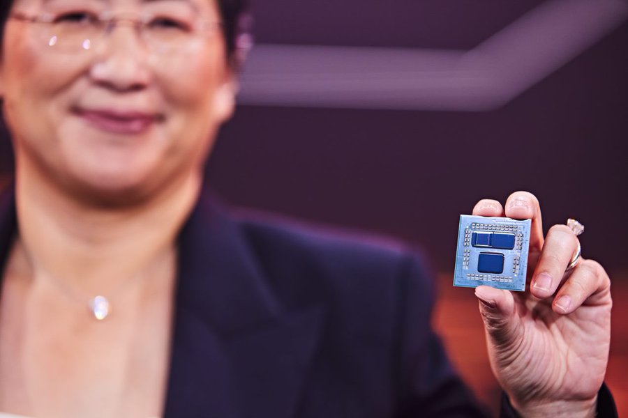
TSMC's 3DFabric portfolio includes brand-new technology, like system-on-integrated-chips (SoIC), which underpins the 3D V-Cache tech in AMD's Milan-X and Ryzen 7 5800X3D processors that came out this year.
The portfolio also includes older technologies: integrated-fan-out and chip-on-wafer-on-substrate (CoWoS), which have received new iterations over the past several years. Those using CoWoS include Nvidia and Amazon Web Services.
- AMD was right about chiplets, Intel's Gelsinger all but says
- Economic cold war looms as Chinese chipmakers feel sting of US trade restrictions
- Samsung, TSMC in US patent infringement investigation
- TSMC downgraded as analysts warn of worst slump in a decade
Representatives from AMD, Nvidia, and AWS gave support for the new alliance, which is one of several set up by TSMC as part of its Open Innovation Platform initiative.
"We've already seen the benefits of working with TSMC and its [Open Innovation Platform] partners on the world's first TSMC-SoIC-based CPUs, and we're looking forward to collaborating even more closely to drive the development of a robust chiplet stacking ecosystem for future generations of energy-efficient, high-performance chips," said AMD executive Mark Fuselier.
TSMC is standing up the new alliance as Intel hopes to entice chip designers to use its own advanced packaging technologies through the rival chipmaker's Intel Foundry Services business. A month ago, Intel CEO Pat Gelsinger said he believes the company's EMIB and Foveros 2D and 3D multi-die packaging technologies are key to extending the life of Moore's Law.
Meanwhile, Samsung, TSMC's largest foundry competitor, has launched a task force to build new advanced packaging solutions to become competitive in the space.
While the pieces are coming together to let more chip designers manufacture chips with advanced packaging, there is still much work to do in other areas. This includes standardizing the interconnect technology necessary to move data between chiplets on multi-die packages.
Most recently, TSMC and several other major chip companies formed a consortium around Universal Chiplet Interconnect Express, a new standard developed by Intel that aims to do for chiplets what PCI-Express did for peripheral devices that slot into computer motherboards. ®
From Chip War To Cloud War: The Next Frontier In Global Tech Competition
The global chip war, characterized by intense competition among nations and corporations for supremacy in semiconductor ... Read more
The High Stakes Of Tech Regulation: Security Risks And Market Dynamics
The influence of tech giants in the global economy continues to grow, raising crucial questions about how to balance sec... Read more
The Tyranny Of Instagram Interiors: Why It's Time To Break Free From Algorithm-Driven Aesthetics
Instagram has become a dominant force in shaping interior design trends, offering a seemingly endless stream of inspirat... Read more
The Data Crunch In AI: Strategies For Sustainability
Exploring solutions to the imminent exhaustion of internet data for AI training.As the artificial intelligence (AI) indu... Read more
Google Abandons Four-Year Effort To Remove Cookies From Chrome Browser
After four years of dedicated effort, Google has decided to abandon its plan to remove third-party cookies from its Chro... Read more
LinkedIn Embraces AI And Gamification To Drive User Engagement And Revenue
In an effort to tackle slowing revenue growth and enhance user engagement, LinkedIn is turning to artificial intelligenc... Read more