
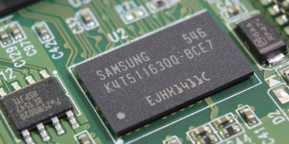
Samsung To Sling 2nm Silicon In 2025, 3nm Process Running A Little Late
Samsung has added a 2nm process node to its foundry roadmap, and said products built with the new tech should go in sale in 2025.
Whenever it lands, the chips will use the gate-all-around (GAA) technology the South Korean giant debuted in 2019. As The Register previously detailed, GAA is an attempt to pack more transistors onto silicon dies.
GAA is needed because today's technique used to increase density – involving fin-shaped field-effect transistors (FinFETs) – relies on having the transistor gate structure poking up a bit like a fish’s fin. That FinFET design loses its performance benefits, and become unattractive to engineers, as the devices are reduced in size, which is well and truly happening as leading-edge manufacturing processes head to 5nm and 3nm nodes.
As its name suggests, GAA moves the transistor channel up into the gate fin so that the gate material surrounds the channel, increasing the contact area and getting the manufacture of efficient, densely packed semiconductors back on track. Samsung, IBM, and TSMC are all working on GAA tech.
The Korean giant calls its effort Multi-Bridge-Channel FET (MBCFET), and says its first-generation 3nm node using the technology will deliver "up to 35 per cent decrease in area, 30 per cent higher performance or 50 per cent lower power consumption compared to the 5nm process."
"Three-nanometre's logic yield is approaching a similar level to the 4nm process, which is currently in mass production," the biz announced at its annual Foundry Forum yesterday.
Samsung previously said it will debut the 3nm process node in 2021. Now it's saying first-gen 3nm products will arrive in the first half of 2022, with a more refined version due the following year.
The company has also revealed that a 2nm process node – again based on MBCFET – "is in the early stages of development with mass production in 2025."
While we wait for that, Samsung has also tickled its 17nm process by adding a 3D transistor architecture it says will improve power consumption, and boost performance by almost 40 per cent compared to the company's 28nm process. The chaebol has in addition paid some attention to its 14nm process "to support 3.3V high voltage or flash-type embedded MRAM (eMRAM) which enables increased write speed and density."
5G is also on Samsung's radar, with 8nm platforms enhanced in ways that ensure the Korean giant can deliver products suited to mmWave RF applications.
- Globalfoundries files for IPO
- Samsung is planning to reverse-engineer the human brain on to a chip
- South Korea surfs silicon shortage to record tech exports
Samsung has made massive investments in foundry capacity. Like other chipmakers, it hopes to cash in on long-term demand for semiconductors and build more resilient supply chains less dependent on input from China – to avoid geopolitical entanglements.
If Samsung can hit its 2025 timeline for 2nm it will deliver a year or so after Taiwan's TSMC plans to mass produce its own silicon at that node. Speaking of TSMC, it hopes to roll out 3nm node parts in volume in the latter-half of next year.
Meanwhile, IBM is hyping up its own 2nm design; Big Blue will need a foundry like Samsung or Intel to make that technology a reality, though.
And, to reiterate, the stated size of a silicon manufacturing process doesn't really matter, because the various elements on an actual die will be larger than the name implies. Intel recently changed the names of its manufacturing processes accordingly, to monikers like "Intel 3" and "20A," in which the A is short for ångström – a unit of length equal to 0.1 nanometres. ®
Booknote
A reader has pointed out that the International Union of Pure and Applied Chemistry's Gold Book – the definitive Compendium of Chemical Terminology – insists the official contraction of ångströms is Å. The Register is eager to be cc'ed on any correspondence between the union and Intel's branding police over this matter.
From Chip War To Cloud War: The Next Frontier In Global Tech Competition
The global chip war, characterized by intense competition among nations and corporations for supremacy in semiconductor ... Read more
The High Stakes Of Tech Regulation: Security Risks And Market Dynamics
The influence of tech giants in the global economy continues to grow, raising crucial questions about how to balance sec... Read more
The Tyranny Of Instagram Interiors: Why It's Time To Break Free From Algorithm-Driven Aesthetics
Instagram has become a dominant force in shaping interior design trends, offering a seemingly endless stream of inspirat... Read more
The Data Crunch In AI: Strategies For Sustainability
Exploring solutions to the imminent exhaustion of internet data for AI training.As the artificial intelligence (AI) indu... Read more
Google Abandons Four-Year Effort To Remove Cookies From Chrome Browser
After four years of dedicated effort, Google has decided to abandon its plan to remove third-party cookies from its Chro... Read more
LinkedIn Embraces AI And Gamification To Drive User Engagement And Revenue
In an effort to tackle slowing revenue growth and enhance user engagement, LinkedIn is turning to artificial intelligenc... Read more