
DRAM, It Stacks Up: SK Hynix Rolls Out 819GB/s HBM3 Tech
Korean DRAM fabber SK hynix has developed an HBM3 DRAM chip operating at 819GB/sec.
HBM3 (High Bandwidth Memory 3) is a third generation of the HBM architecture which stacks DRAM chips one above another, connects them by vertical current-carrying holes called Through Silicon Vias (TSVs) to a base interposer board, via connecting micro-bumps, upon which is fastened a processor that accesses the data in the DRAM chip faster than it would through the traditional CPU socket interface.
Seon-yong Cha, SK hynix's senior vice president for DRAM development, said: "Since its launch of the world's first HBM DRAM, SK hynix has succeeded in developing the industry's first HBM3 after leading the HBM2E market. We will continue our efforts to solidify our leadership in the premium memory market."

Schematic diagram of high bandwidth memory
The previous generations were HBM, HBM2 and HBM2E (Enhanced or Extended), with JEDEC developing standards for each. It has not yet developed an HBM3 standard, which means that SK hynix might need to retrofit its design to a future and faster HBM3 standard.

The rightmost column its a possible future HBM3 standard and the empty column is our guess-timated SK hynix HMB3 I/O speed
The 819GB/sec speed is a 78 per cent increase on the firm's HBM2e chip speed of 460GB/sec. SK hynix used 8 x 16Gbit layers in its 16GB HBM2e chip. The HBM3 chip comes in 24GB and 16GB capacities with the 24GB chip having a 12-layer stack.
The company says its engineers ground their DRAM chip height to approximately 30 micrometer (μm, 10-6m), equivalent to a third of an A4 paper's thickness, before vertically stacking up to 12 of them using TSV technology.
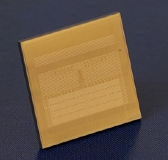
Underside (Interposer side) of the SK hynix HBM3 chip
Producing an HBM3 chip is only half, so to speak, of what needs to be done, since it has to be fixed to an interposer-processor combo and that needs to be built to accommodate the memory component.
Building an HBM-interposer-processor combo will generally only be done for applications that need more memory capacity and speed than that provided by industry-standard server CPUs and their socket scheme. That means supercomputers, HPC systems, GPU servers, AI systems and the like where the expense and specialisation (restricted market) is worthwhile.
We might expect systems using SK hynix's HBM3 to appear after mid-2022 and in 2023. ®
From Chip War To Cloud War: The Next Frontier In Global Tech Competition
The global chip war, characterized by intense competition among nations and corporations for supremacy in semiconductor ... Read more
The High Stakes Of Tech Regulation: Security Risks And Market Dynamics
The influence of tech giants in the global economy continues to grow, raising crucial questions about how to balance sec... Read more
The Tyranny Of Instagram Interiors: Why It's Time To Break Free From Algorithm-Driven Aesthetics
Instagram has become a dominant force in shaping interior design trends, offering a seemingly endless stream of inspirat... Read more
The Data Crunch In AI: Strategies For Sustainability
Exploring solutions to the imminent exhaustion of internet data for AI training.As the artificial intelligence (AI) indu... Read more
Google Abandons Four-Year Effort To Remove Cookies From Chrome Browser
After four years of dedicated effort, Google has decided to abandon its plan to remove third-party cookies from its Chro... Read more
LinkedIn Embraces AI And Gamification To Drive User Engagement And Revenue
In an effort to tackle slowing revenue growth and enhance user engagement, LinkedIn is turning to artificial intelligenc... Read more