
AMD Slaps Together A Silicon Sandwich With MI300-series APUs, GPUs To Challenge Nvidias AI Empire
AMD is pushing advanced packaging and chiplets to the limit with the launch of its Instinct MI300-series accelerators, part of a quest to close the gap with rival Nvidia in the AI arena and bolster its standing in the high performance computing (HPC) community.
When the generative AI hype train left the station in late 2022 amid the launch of ChatGPT, AMD lacked a competitive answer. Its MI250X, which powers the number-one-ranked Frontier supercomputer, was stellar at crunching highly precise FP64 mathematics. But it came up short next to Nvidia's H100 in lower precision workloads common in AI training and inference.
The MI250X was capable of hitting just shy of a 100 teraFLOPS at FP64 but could only manage 383 teraFLOPS of FP16 or BF16, putting it just ahead of Nvidia's A100 — if you ignore sparsity of course. Next to the H100, however, the MI250X came up short. At FP8, Nvidia's flagship could top 1,979 teraFLOPS in its SXM form factor and with sparsity its closer to four petaFLOPS of performance.
With the launch of the Instinct MI300A APUs and MI300X GPUs this week, AMD aims to rectify this performance deficit with modular accelerators tuned for HPC, AI training, and inference. And going off AMD's performance claims, it looks like it has done just that.
AMD says its MI300X GPUs not only match but exceed the speed of Nvidia's H100, with FP8 performance of 2.6 petaFLOPS. We're told the MI300-series parts follow a standard 2:1 advantage — the same we see from Nvidia.

AMD claims the Instinct MI300X will deliver up to 32 percent higher performance in AI workloads than the Nvidia H100. - Click to enlarge
In terms of sheer FLOPS, that makes the MI300X 32 percent faster than Nvidia's H100. However, the MI300-series part's biggest advantage still comes down to memory.
The MI300X not only has more of it but it's also faster, coming in at 5.2TB/s of bandwidth compared to 3.35TB/s for the H100. Of course, that lead diminishes somewhat when you consider the recently announced H200 will apparently have 141GB of HBM3e at 4.8TB/s of bandwidth — 4.9TB/s in the case of Nvidia's Grace-Hopper superchip. Still AMD holds the lead here.
This translates into substantial performance lead when it comes to AI inferencing, according to AMD, with the MI300X claiming a 1.6x lead over the H100 in terms of token throughput in the Bloom 176 billion parameter large language model and a 1.4x lead in terms of latency for Meta's Llama 2 70B model. When it comes to AI training, meanwhile, AMD says the MI300X will be "competitive" with performance on par with Nvidia's H100.

AMD's Instinct MI300A promises up to 1.8x higher performance than the Nvidia H100 in HPC workloads - Click to enlarge
For HPC workloads, meanwhile, AMD's MI300A's combination of Zen 4 CPU cores and CDNA 3 graphics cores is rated for 122.6 teraFLOPS of double precision performance — 1.8x that of the H100. However, thanks to its coherent memory architecture, AMD suggests that customers could see as much as a four-fold improvement in performance compared to the H100 in benchmarks like OpenFoam Motorbike.
As with all vendor supplied numbers, we recommend taking AMD's claims with a grain of salt. Having said that, how AMD managed to squeeze all that performance from the chip is just as important and arguably the more interesting element to the launch.
AMD brings Epyc modularity to Instinct
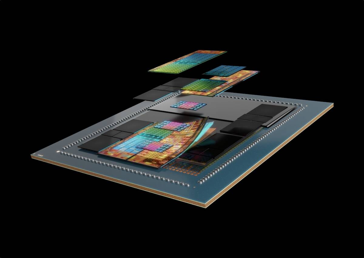
AMD's MI300-series parts are unlike anything we've seen from the chip biz before, both in terms of packaging and architecture.
Considering the ongoing hype around LLMs and generative AI, we'll kick things off with AMD's new GPU for AI training and inference, the MI300X, since it's the simpler of the two.
Compared to its predecessor, the MI250X, the MI300X is a far more complex bit of kit, sticking together 12 I/O and GPU dies into something of a silicon sandwich. At the heart of the chip are eight XCDs — what AMD calls its GPU dies.
MI300 meshes 24 Zen 4 cores, six CDNA 3 GPU dies and 128GB of HBM3 memory onto a single package aimed at HPC workloads - Click to enlarge
Each of these chiplets features 40 CDNA 3 compute units backed by 4MB of shared L2 cache, although only 38 are actually active. In total, the MI300X packs 304 CDNA 3 compute units along with 192GB of HBM3 memory into a single package.
This vertical integration is possible thanks to a number of advanced 2.5D and 3.5D packaging techniques like TSMC's chip-on-wafer-on-substrate (CoWoS). These techniques are nothing new for AMD. The company was arguably responsible for popularizing the technique in its Epyc CPUs using multiple smaller, higher yielding dies into a single logical unit.
Starting from the top and working our way down, two GPU chiplets (XCDs) are stacked atop each of the four I/O dies using a technique similar to the one used in AMD's X-chips to attach more SRAM. The I/O dies are then bonded to a silicon interposer connected to the organic substrate using TSMC CoWoS.
Just like on Epyc, memory is connected to the MI300's I/O die rather than the CPU itself. But, instead of your typical DDR5 memory controllers going out to a couple of DIMMs on the motherboard, each HBM3 stack is attached using TSMC's 2.5D packaging tech for maximum bandwidth.

AMD Instinct MI300-series accelerators use a combination of 2.5D and 3.5D packaging to create a dense compute sandwich. - Click to enlarge
AMD's APU, the MI300A, takes this formula to new extreme by swapping out two of the CDNA 3 GPU chiplets in favor of a trio of CPU dies totaling 24 Zen 4 cores and carrying 128GB of HBM3 memory.
And If you're wondering, these are the same CCDs found on AMD's Epyc 4 chips launched late last autumn. Early renderings of the MI300A had us puzzled as to whether they were using a custom CPU chiplet or not.
APUs — what AMD has long called chips that featuring both CPU and GPU cores — have been a key component of AMD's desktop and mobile processor families for years. The MI300A marks the first time AMD has applied this approach to a datacenter chip and unlike most APUs we've seen from the House of Zen to date, this one isn't monolithic and is aimed solidly at the HPC market.
The benefit of this compute and IO sandwich is extremely high performance communication between the dies and memory. As the chart below illustrates, two HBM3 stacks deliver 1.33TB/s of bandwidth to each of the four IODs, which can communicate with each other at between 1.2TB/s and 1.5TB/s in each direction. This allows each IOD to feed up to two GPU tiles at 2.1TB/s each.

AMD is pushing some serious bandwidth between the MI300's chiplets with bandwidth measured in terabytes per second. - Click to enlarge
In fact, the biggest bottleneck in the entire architecture is for data going off package. The four I/O dies provide a total of 1Tb/s of bandwidth — 512 GB/s in either direction — for communications between accelerators, hosts, or peripherals depending on the configuration. According to AMD, this allows its Mi300A APU to support four socket configurations while the MI300X GPU will support carrier boards with up to eight sockets.
Cramming all of that performance into such a dense package does come at the cost of higher power consumption, but it's not nearly as bad as we'd feared. Initial performance disclosures suggested the chips might consume as much as 850W. Instead, the MI300X is rated for 750W, about 150W more than its predecessor, but just 50W more than the H100. The MI300A, meanwhile, appears to have a variable TDP ranging from 550W to 760W.
The competitive landscape
AMD is hardly the first to talk about building datacenter APUs. Intel's Falcon Shores was originally envisioned as an XPU — because of course Chipzilla can't just call it an APU — with a flexible arrangement of CPU and GPU cores and tiles.
However, with the cancellation of Ponte Vecchio's successor Rialto Bridge, Intel abandoned the concept, with Jeff McVeigh, VP of Intel's supercomputing group, arguing at the time that the "push to integrate a CPU and GPU into an XPU was premature." Falcon Shores has since been reimagined as a standard GPU integrating IP from Inte's Habana AI division and is due out in 2025.
Then there's Nvidia's Grace-Hopper Superchip which pairs an Arm processor with 72 Neoverse V2 cores with an H100 GPU die, 512GB of LPDDR5x memory, and either 96GB of HBM3 or 144GB of HBM3e.
- AMD SEV OMG: Trusted execution in VMs undone by bad hypervisors' cache meddling
- Nvidia intros the 'SuperNIC' – it's like a SmartNIC, DPU or IPU, but more super
- Tech world forms AI Alliance to promote open and responsible AI
- Thirty-nine weeks: That's how long you'll be waiting for an AI server from Dell
While it may be tempting to draw comparisons between that chip, now called the GH200, to AMD's MI300A, there are a couple of notable differences worth pointing out.
The way the two chips CPUs and GPUs are interconnected is very different. Rather than the silicon-to-silicon die stacking we see on the MI300-series parts, Nvidia's GH200 uses its 900GB/s NVLink-C2C interconnect to bridge the two chips. While NVLink is fast, it's not even close to the TB/s of bandwidth AMD is pushing through its dies on MI300. With that said, for off-package communications, NVLink is still a hair faster at 900 GB/s vs the 896GB/s enabled by the MI300-series parts.
Another key difference relates to memory domains. Nvidia's GH200 uses DRAM for the CPU and HBM for the GPU. This provides the advantage of capacity, data still has to be copied from one to the other before it can be processed. The MI300A, on the other hand, shares its memory between the CPU and GPU seamlessly. Both processors can read, write, and operate on the same pool of HBM eliminating the need for costly copy operations.
The cost of this approach, as we've already explored, is complexity. MI300 is without a doubt a more complicated chip, at least in terms of packaging. Nvidia's GH200 is simpler, but potentially less efficient when it comes to data movement. Which approach is inherently better isn't clear, and will likely depend on the situation the hardware is used for.
Looking at the broader GPU and AI accelerator market MI300X will have to compete with Nvidia's recently announced H200 GPU, which offers higher memory bandwidth than the H100 thanks to the shift to faster HBM3e kit. According to Nvidia's roadmap, that chip is really a placeholder for Nvidia's next generation B100 coming out in 2024.
The MI300X will also compete with Intel's long-awaited Gaudi 3 AI accelerator in 2024. While details are thin, Intel claims it will deliver a 4x improvement in brain float 16 performance and 50 percent increase in memory capacity and bandwidth.
Availability and deployment
On the topic of availability, both APU and GPU versions of the MI300 are already making their way out to customers. Some of the earliest adopters are Microsoft, Oracle, and the DoE's Lawrence Livermore National Labs.
Last month, Microsoft Azure announced a MI300X powered VM. These instances boast eight accelerators totaling 1.5TB of HBM3 memory backed by 400Gb/s Infiniband networking to each of the cards.
Oracle will also make AMD's MI300X available to rent alongside its massive cluster of Nvidia A100 and H100 accelerators.
On the HPC side, work on Lawrence Livermore National Lab's MI300A-powered El Capitan supercomputer is already under way. The system, which our sibling site The Next Platform took an early look at in June, is due to come online later next year promises 2 exaFLOPS of peak performance.
Given the extreme demand for AI accelerators and the advanced packaging tech involved in these chips, the capacity for which is already constrained, we expect it may be difficult to get your hands on either the MI300A or X varients unless you're a government agency or hyperscale cloud provider.
Nonetheless, several major OEMs have announced their support for the chips, including, Hewlett Packard Enterprise, Lenovo, Supermicro, Eviden, Gigabyte and others. ®
From Chip War To Cloud War: The Next Frontier In Global Tech Competition
The global chip war, characterized by intense competition among nations and corporations for supremacy in semiconductor ... Read more
The High Stakes Of Tech Regulation: Security Risks And Market Dynamics
The influence of tech giants in the global economy continues to grow, raising crucial questions about how to balance sec... Read more
The Tyranny Of Instagram Interiors: Why It's Time To Break Free From Algorithm-Driven Aesthetics
Instagram has become a dominant force in shaping interior design trends, offering a seemingly endless stream of inspirat... Read more
The Data Crunch In AI: Strategies For Sustainability
Exploring solutions to the imminent exhaustion of internet data for AI training.As the artificial intelligence (AI) indu... Read more
Google Abandons Four-Year Effort To Remove Cookies From Chrome Browser
After four years of dedicated effort, Google has decided to abandon its plan to remove third-party cookies from its Chro... Read more
LinkedIn Embraces AI And Gamification To Drive User Engagement And Revenue
In an effort to tackle slowing revenue growth and enhance user engagement, LinkedIn is turning to artificial intelligenc... Read more